- A6001C17 Advances in Animal Production Science Assignment Brief 2026 | HAU
- SOCI5270 Contemporary Sociological Theory Essay Assessment 2026 | UOK
- 4BE002 The Innovative Business Assignment Brief 2026 | University of Wolverhampton
- CIPD Level 5 5LD01 Support Informal and Self-Directed Learning Assessment Brief 2026
- COM4016 Productivity and Collaboration Tools for Learning and Work Assessment Brief 2026 | Arden University
- CA6060 Financial Decision-Making in Context for Aviation Assignment 2 Question 2026
- NCFE CACHE Level 3 Diploma for Working in the Early Years Sector Assessment Brief 2026
- CRN 63466 / CRN 63467 Statutory Valuation Level 7 Assessment Brief 2026 | USM
- BSM24105 Operations and Project Management Assessment Brief 2026 | RUL
- Professional Communication Assessment 1 Semester 2, 2026 | UGM
- LAW7128 Conflict Resolution in Business Assignment Brief 2026 | BCU
- MLA604 Maritime Operations Assessment Brief Jan 2026 | MLA College
- HS7008 Research Methods in Public Health Summative Assignment 2026 | UEL
- MAR020-1 Introduction to Digital Marketing and Analytics Assignment 1 Brief 2026 | UOB
- LCBB5014 Data Handling and Business Intelligence Assignment Brief 2026 | UOW
- 6BM040 Honours Research Project Assessment Brief 2026 | University of Wolverhampton
- A334 English Literature from Shakespeare to Austen Tutor-Marked Assignment 03, 2026 | OU
- ADV767 Advanced Clinical Reasoning in Musculoskeletal Conditions Assessment Brief 2026 | UOP
- IS2184 Information Systems Management Individual Assignment 2026 | UOL
- MK7050 Principles and Practices of International Business Assessment Brief 2026
Pearson BTEC Level 5 Higher National Diploma in Engineering : Unit 4019 Electrical and Electronic Principles Assignment Final Report with Practical Labs, Circuit Analysis & Simulations
| University | Uxbridge College (UC) |
| Subject | Unit 4019 Electrical and Electronic Principles |
ASSIGMENT PART 1
Problem 1:
In Physical lab 2, Activity II – “Find the internal resistance of the battery”, you tried to find the internal resistance (R1) of a 1.5V battery.
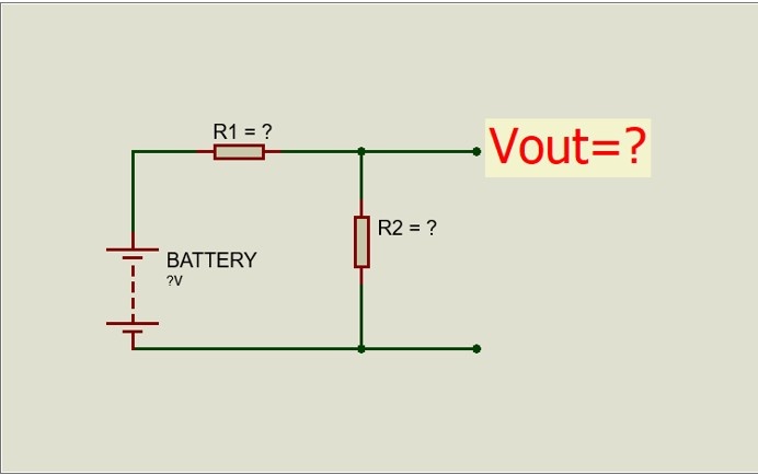
Figure 1. Schematic circuit to find internal resistance, physical lab 2.
Your lecturer MUST confirm that you did this in the lab.
Referring to Figure 1,
- Show the pictures of your assembled circuit on breadboard.
- Show your measured value for the battery voltage (Vbattery) and R2.
- Explain the operation of that circuit. In particular,
– Using Ohm’s law and voltage division, calculate R1.
– Show your calculation for R1.
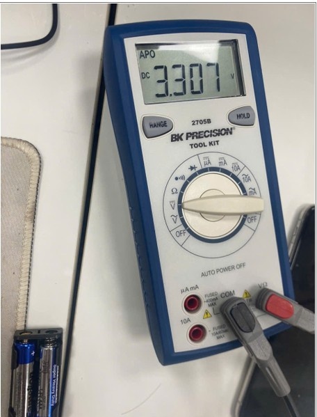
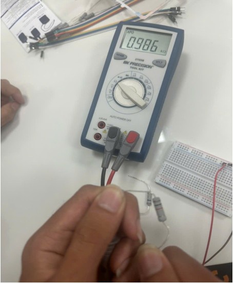
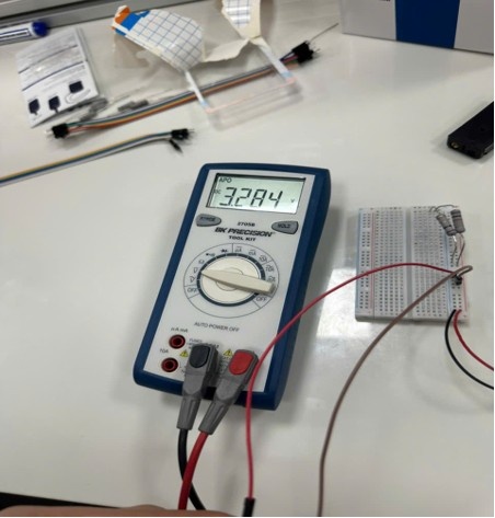
Measured Values:
Battery voltage: Vbattery = 3,307 V
Resistor: R2 = 986Ω
Output voltage: Vout = 3,284V
Circuit structure analysis: The circuit is a simple voltage divider. The internal resistance R1 can be calculated.
1.1) Find R1:
Apply Voltage Division rule:
Formula: Vout = Vbattery × R_2/(R_2+R_1 )
Vout/Vbattery= R_2/(R_2+R_1 ) => R1 = R2(V_battery/Vout-1) R1 = 986(3,307/3,284-1) ≈ 6,9056Ω
Do You Need Assignment of This Question
Problem 2:
In Physical lab 2, Activity III – “Resistor in series and in parallel”, you experimented a circuit with resistors in series and in parallel. Applying several laws of circuit theory, you will now explain the operation of this circuit, by answering the following questions:
a) Series resistors (Figure 2)
Figure 2. Schematic circuit of resistors in series, physical lab 2.
Your lecturer MUST confirmed that you did this in the lab.
Referring to Figure 2,
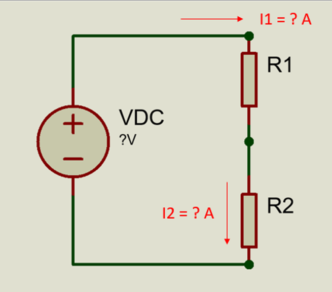
i) Show pictures of your assembled circuit on breadboard.
ii) Show your measured value for I1, I2, R1, R2 and VDC.
iii) Using Ohm’s law, calculate V1 = I1 × R1 and V2 = I2 × R2. Are your results the same as the measured values V1 and V2?
Measured Values:
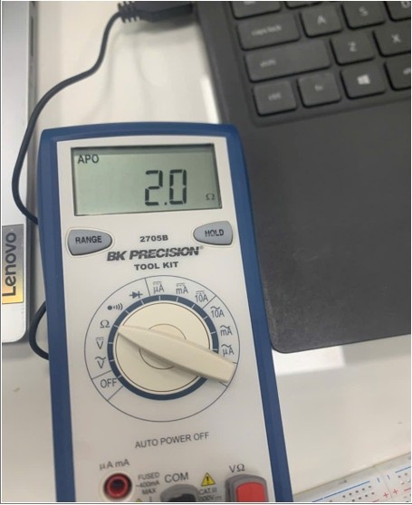
Total resistance: R = R1 + R2 = 2 + 986 = 988Ω
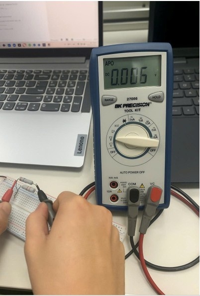
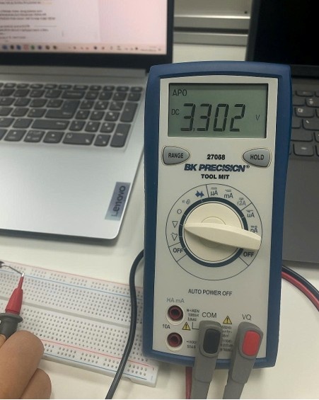
Total voltage: VDC = V1 + V2 = 0,003 + 3,305 = 3,308V
Current of circuit: I = VDC/R = 3,308/988 ≈ 0,00335A
Check again with Ohm’s Law:
V1 = I × R1 = 0,00355 × 2 ≈ 0,006V
V2 = I × R2 = 0,00355 × 988 ≈ 3,302V
I1 = V1/R1 = 0,006/2 = 0,003A
I2 = V2/R2 = 3,302/986 ≈ 0,00335A
b) Parallel resistors (Figure 3)
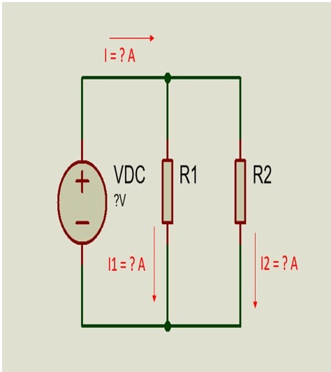
Figure 3. Schematic circuit of resistors in parallel, physical lab 2.
Your lecturer MUST confirmed that you did this in the lab.
Referring to Figure 3,
i) Show pictures of your assembled circuit on breadboard.
ii) Show your measured value for I1, I2, R1, R2 and VDC.
iii) Is I = I1 + I2? Show your calculation. What law is this?
iv) Is /1 = R2/R1+R2*I ? Show your calculation. What law is this?
Battery voltage: VDC = Vbattery = 3,307 V
Resistor: R1 = 2Ω
Resistor: R2 = 986Ω
Calculated values included in document:
Total resistance: R = R1R2/(R1+R2)= (2×986)/(2+986)= 493/247Ω
Apply Ohm’s Law: I = V/R = (3,307)/(493/247) ≈ 1,656853A
Check if I = I1 + I2
VDC = V1 = V2 = 3,307V( 2 parallel resistors)
I1 = V1/R1= (3,307)/2= 1,6535A
I2 = V2/R2= (3,307)/986 ≈ 0,003353A
Total Current I = I1 + I2 = 1,6535 + 0,003353 = 1,656853A
So the summary is correct
Check if I1= R2/(R1+R2)×I
I1 = V1/R1= (3,307)/2= 1,6535A
R2/(R1+R2)×I = R2/(R1+R2) × V/R= (2×986)/(2+986) × (3,307)/(493/247) = 1,6535A
So the equation is correct
Buy Answer of This Assessment & Raise Your Grades
Problem 3:
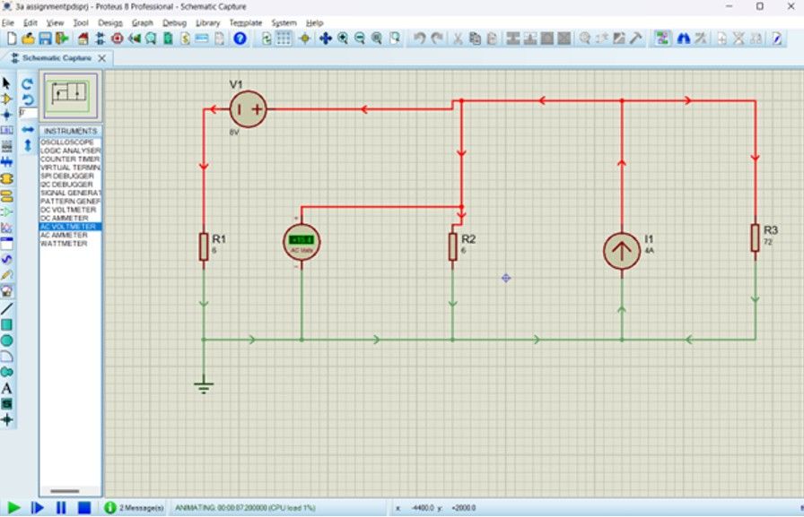
Explain the operation of the circuit in Figure 4:
- Apply Ohm’s law, Kirchhoff’s laws and Mesh or Nodal analysis
- Find V0 and the power over the 3𝝮 resistor in the circuit of Figure 4
- Show your calculation
- Use Proteus to check your result. Add pictures of your simulated circuit and simulated result.
n is a random number given by the lecturer for each student.
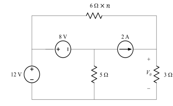
Figure 4
Give n number: 21
v_1=12V,v_2=v_1-8=4V
I=I_1+I_2
I_2=2+I_3
=>I=I_1+I_3+2(1)
Apply Ohm’s Law and given data
=>I_1=(v_1-v_0)/R=(12-v_0)/126 (2)
I_3=v_2/5=4/5
v_0=(3I_1+2)(3)
Replace (3) with (2)
v_0=3((12-v_0)/126+2)
=>v_0=264/43 V
P=v^2/R=(264/43)^2/3≈12,6W
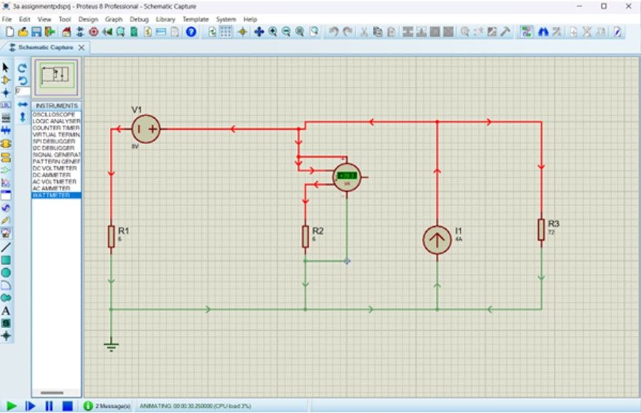
Problem 4:
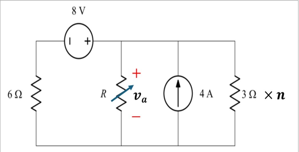
Figure 5
In the circuit shown in Figure 5, where n is a random number given by lecturer for each student, R is a Variable resistor.
Examine the circuit, then answer the following questions about its operation:
In case R = 6𝝮,
Use superposition to obtain va in the circuit of Figure 5.
Show your work and use Proteus to check the value of va.
Add pictures of your simulated circuit and simulated result.
Circuit has:
Voltage source 8V
Current source 4A
R1 = 6(Variable resistor), R2 = 3.21 = 63(n=21)
Considering 8V (turn off 4A – replacing with a short circuit)
1/R_z =1/R_1 +1/R_2 =1/6+1/63=23/126⇒R_z=126/23 Ω
R_t=R_z+R_1=126/23+6=264/23 Ω
Apply Ohm’s law:
I=V/Rt=8/(264/23)=23/33 A
V_(a_1 )=R_z×I=126/23×23/33=42/11 V
Considering 4A (turn off 8V – replacing with a short circuit)
V_(a_2 )/6+V_(a_2 )/6+V_(a_2 )/63=4⇒V_(a_2 )=126/11 V
Using the superposition theorem, the total voltage is:
V_a=V_(a_1 )+V_(a_2 )=42/11+126/11=15,27V
b.Compute the value of R that results in maximum power transfer in the circuit of Figure 5.
Find the maximum power.
Show your work and use Proteus to check your answer.
Add pictures of your simulated circuit and simulated result.
Using Thevenin’s Theorem
Replace the 8V voltage source Short circuit (wire)
Replace the 4A voltage source Open circuit
Thevenin resistance:
R_th=(6×63)/(6+63)=126/23 Ω
Thevenin voltage:
(v-v_th)/R_1 +I=v_th/R_2 ⇒(8-v_th)/6+4=v_th/63⇒v_th≈29.21739V
Maximum power transfer in the circuit:
P_(m=(v_th )^2/(4R_th ))=〖29,22〗^2/(4.126/23)=38,96W
Problem 5:
Analyse the RLC circuit below (Figure 6) and:
- Find the steady-state voltage over the inductor and the current going through the inductor.
- Show your work.
Each student receives a different ω value (rad/s) from the lecturer.
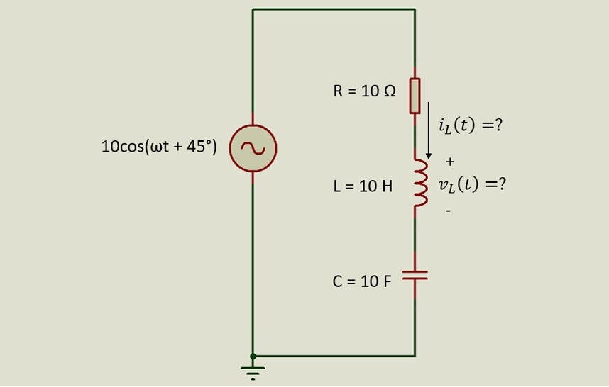
Circuit has:
R = z_R = 10Ω
L = 10H
C = 10F
V(t) = 10cos(ωt + 45^0) = V_S = 10∠45° (V)
ω = 21(rad/s)
Impedance of inductor: z_L= jωL =j .21.10 = j210Ω
Impedance of capacitor: z_C=1/jωC= 1/(j⋅21.10)=-1/j210≈ -j0.004761904761904762Ω
Equivalent impedance: z_eq=z_R+z_L+z_C= 10 + j210 – j0.004761904761904762Ω
= 10 + j209.9952380952381(Ω)
Find i_L (t):
Modulus:|Z|= √(Z^2+X^2 )= √(10^2+(209,9952)^2 ) = 210,233Ω
Phase angle of the sum:∅=〖tan〗^(-1) (X/R)= 〖tan〗^(-1) (209,9952/10)≈87,27°
i_L (t)= V_S/z_eq = (10∠45°)/(210.233∠87,27°) ≈ 0,047566∠-42,27°
Find v_L (t):
v_L (t) = I.Z = 0,047566∠-42,27°.240 = 9.98886∠47,73°
Are You Looking for Answer of This Assignment or Essay
Problem 6:
In Figure 7 below, analyse the combined RLC circuit and determine the phasor voltage V.
Show your work.
In the process:
- Use Kirchhoff’s laws, Ohm’s law and Mesh or Nodal analysis for AC circuit
- Transform between complex number and phasor
Each student receives a different n value from the lecturer
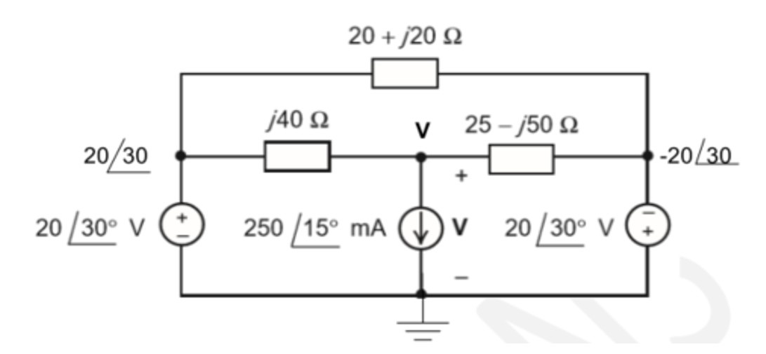
Given
n = 21
V_L = 20∠30°
V_R = 20∠-30°
I = 250∠15° mA = 0,25∠15°A
Z_1 = 20 + j20 (Ω)
Z_2= n.j40 = 21.j40 = j840 (Ω)
Z_3 = 25 – j50 (Ω)
Apply KCL at node V:
Current through: Z_1: I_1 = (V-(20∠〖30〗^0 ))/Z_1 =(V-(20∠〖30〗^0 ))/(20+j20)
Z_2: I_2 = v/Z_2 = V/j840
Z_3: I_3 = (V-(20∠〖30〗^0 ))/Z_1 = (V-(20∠-〖30〗^0 ))/(25+j50)
Total equation at node V: I_1 + I_2 + I_3 – I = 0
(V-(20∠〖30〗^0 ))/(20+j20) + V/j840 + (V-(20∠-〖30〗^0 ))/(25+j50) – 0,25∠15° = 0
V((1-(20∠30^0 ))/(20+j20) + 1/j840 + (1- (20∠-30^0 ))/(25+j50)) – 0,25∠15° = 0
V(1/(20+j20) + 1/j840 + 1/(25+j50)) = ((20∠30^0 ))/(20+j20) + ((20∠-30^0 ))/(25+j50) + 0,25∠15°
Compute the complex quatities:
1/(20+j20)= (20- j20)/((20+j20)(20-j20))=(20- j20)/800= 0,025 – j0,025
1/j840 ≈ -j1.190476.10^(-3)
1/(25+j50) = (25- j50)/((25+j50)(25-j50)) = (25- j50)/3125 = 8. 〖10〗^(-3)+ 16. 〖10〗^(-3)
Problem 7:
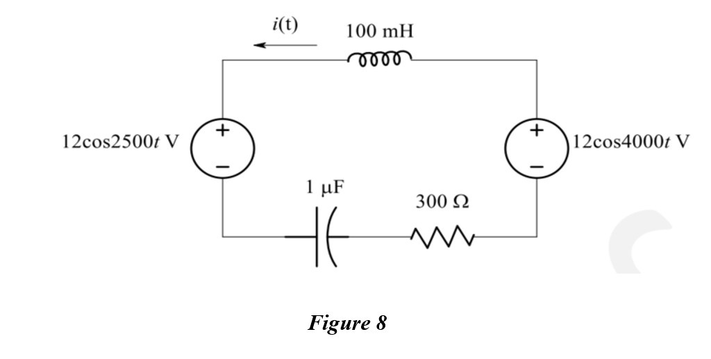
Evaluate the operation and behaviour of the series RLC circuit in Figure 8 by doing the following steps:
- Calculate the damping factor
- Calculate the resonant frequency
- Determine if the circuit is overdamped, critically damped or underdamped
- Determine if the transient response of i(t) will be quick, somewhat quick or slow.
- Determine if there will be resonance in the circuit or not.
Remember to show your calculation and reasoning.
Each student receives a different value of n from the lecturer.
ASSIGNMENT PART 2
Problem 1:
Answer the following questions:
- a) Describe the voltage condition for a PN junction to conduct current. Draw or add picture for the I-V graph of a diode.
- b) Describe the voltage condition for an NPN transistor to conduct current. Illustrate your answer using the NPN transistor symbol.
- c) Describe the voltage condition for a PNP transistor to conduct current. Illustrate your answer using the PNP transistor symbol.
Problem 2:
In Physical lab 5, you already demonstrated the action of diodes by implementing a full-wave rectifier, both in practical and analytical settings.
- a) Show pictures of your assembled circuits on breadboard, and the relevant oscilloscope measurements in Physical lab 5.
Your lecturer MUST confirm that you did the lab.
- b) Based on your assembled circuits in Physical lab 5, explain shortly:
– Which property of the diodes allow us to convert an AC signal to DC signal?
– How did capacitors help smoothing out the circuit?
Problem 3:
Explain the main difference between digital and analogue electronics. Draw or add pictures for analogue and digital signals.
Problem 4:
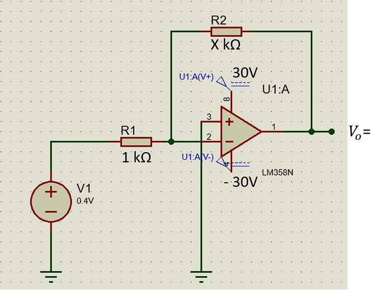
Explain the operation of the inverting amplifier in Figure 1 in analytical setting:
- include calculations
- find the output voltage Vo
Lecturers give different X value for each student.
For practical setting, use Proteus to check your result. Add pictures of your simulated circuit and simulated result.
Figure 1. Inverting amplifier
Problem 5:
The application of “Binary Decoder” to control the lamp system is described in Figure 2. The “Binary Decoder” using Logic gates is described in Figure 3.
Figure 2. Lamp controlling system
Figure 3. Logic circuit of the binary decoder
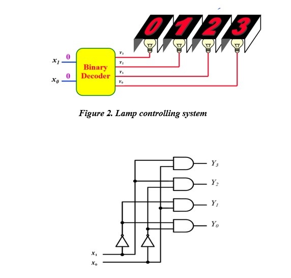
Examine the circuit above:
- Draw the truth table for each output.
- Assuming that the lamps are Active-High, determine the status of the lamps (on or off) when X0 = 1 (High) and X1 =0 (Low).
Problem 6:
- a) Analyse the operation of a PN junction. Your answer must include the concepts of doping, holes, electrons, depletion region, forward bias, and reverse bias.
- b) Analyse the operation of a bipolar NPN transistor work. Your answer must include the concepts of doping, depletion region, forward bias, and reverse bias.
- c) Analyse the operation of a bipolar PNP transistor work. Your answer must include the concepts of doping, depletion region, forward bias, and reverse bias.
Problem 7:
Critique the benefits and drawbacks of using analogue and digital electronic devices using examples.
Problem 8:
- a) When will a diode break down? Explain using the concept of reverse bias, depletion region and current direction.
- b) Zener diode is widely used for its break-down property. Discuss why we DID NOT use Zener diode in Physical lab 5? Use simple semiconductor theory in your answer.
- c) Discuss why we can use BJT transistors to amplify signals? Use simple semiconductor theory in your answer.
Problem 9:
Reflecting on your experience in Physical lab 5,
- a) Evaluate the role of analogue electronic circuits in supplying power to a device.
- b) Evaluate the role of digital electronic circuits in supplying power to a device.
Do You Need Assignment of This Question
Many students find it challenging to apply Ohm’s law, Kirchhoff’s laws, and circuit simulations in their BTEC Level 5 Electrical & Electronic Principles assignments. From lab-based resistor experiments to RLC circuit analysis, linking theory with practical results often causes stress. At Students Assignment Help UK, we provide plagiarism-free, AI-free guidance through Electrical Engineering Assignment Help, ensuring accuracy and clarity. Explore our expert assignment writing services UK today for better results.
Answer